- 您现在的位置:买卖IC网 > Sheet目录340 > MAX15012AASA+ (Maxim Integrated Products)IC DRIVER MOSFET 8-SOIC
175V/2A, High-Speed,
Half-Bridge MOSFET Drivers
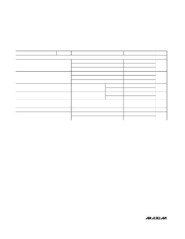
ELECTRICAL CHARACTERISTICS (continued)
(V DD = V BST = +8V to +12.6V, V HS = GND = 0V, T A = T J = -40°C to +125°C, unless otherwise noted. Typical values are at V DD =
V BST = +12V and T A = +25°C.) (Note 2)
PARAMETER
SYMBOL
CONDITIONS
MIN
TYP
MAX
UNITS
SWITCHING CHARACTERISTICS FOR HIGH- AND LOW-SIDE DRIVERS (V DD = V BST = +12V)
C L = 1000pF
7
Rise Time
t R
C L = 5000pF
33
ns
C L = 10,000pF
C L = 1000pF
65
7
Fall Time
t F
C L = 5000pF
33
ns
C L = 10,000pF
65
Turn-On Propagation Delay Time
Turn-Off Propagation Delay Time
t D_ON
t D_OFF
Figure 1, C L = 1000pF
(Note 5)
Figure 1, C L = 1000pF
(Note 5)
CMOS
TTL
CMOS
TTL
30
35
30
35
55
63
55
63
ns
ns
Delay Matching Between Driver-
Low and Driver-High
t MATCH
C L = 1000pF, Figure 1 (Note 5)
2
8
ns
Internal Nonoverlap
1
ns
Minimum Pulse Width Input Logic
(Note 6)
t PW-min
V DD = V BST = 12V
V DD = V BST = 8V
135
170
ns
Note 2: All devices are 100% tested at T A = +125°C. Limits over temperature are guaranteed by design.
Note 3: Ensure that the V DD -to-GND or BST-to-HS transient voltage does not exceed 13.2V.
Note 4: Maximum operating supply voltage (V DD ) reduces linearly from 12.6V to 10.5V with its maximum voltage (V HS_MAX ) increasing
from 125V to 175V. See the Typical Operating Characteristics and Applications Information sections.
Note 5: Guaranteed by design, not production tested.
Note 6: See the Minimum Input Pulse Width section.
4
_______________________________________________________________________________________
发布紧急采购,3分钟左右您将得到回复。
相关PDF资料
MAX15015EVKIT
EVAL KIT FOR MAX15015
MAX15018BASA+
IC MOSF DRVR HALF BRDG HS 8-SOIC
MAX15022EVKIT+
KIT EVAL FOR MAX15022
MAX15025EATB+T
IC GATE DRVR 2CH 16NS 10TDFN-EP
MAX15053EVKIT+
BOARD EVAL FOR MAX15053
MAX15054AUT+T
IC MOSFET DVR HIGH SIDE SOT-23-6
MAX15070BEUT+T
IC MOSFET DRIVER HNM LL SOT23-6
MAX15103EVKIT#
EVAL KIT MAX15103
相关代理商/技术参数
MAX15012AASA+T
功能描述:功率驱动器IC 175V/2A High-Speed Half-B MOSFET Drvr RoHS:否 制造商:Micrel 产品:MOSFET Gate Drivers 类型:Low Cost High or Low Side MOSFET Driver 上升时间: 下降时间: 电源电压-最大:30 V 电源电压-最小:2.75 V 电源电流: 最大功率耗散: 最大工作温度:+ 85 C 安装风格:SMD/SMT 封装 / 箱体:SOIC-8 封装:Tube
MAX15012BASA+
功能描述:功率驱动器IC 175V/2A High-Speed Half-B MOSFET Drvr RoHS:否 制造商:Micrel 产品:MOSFET Gate Drivers 类型:Low Cost High or Low Side MOSFET Driver 上升时间: 下降时间: 电源电压-最大:30 V 电源电压-最小:2.75 V 电源电流: 最大功率耗散: 最大工作温度:+ 85 C 安装风格:SMD/SMT 封装 / 箱体:SOIC-8 封装:Tube
MAX15012BASA+T
功能描述:功率驱动器IC 175V/2A High-Speed Half-B MOSFET Drvr RoHS:否 制造商:Micrel 产品:MOSFET Gate Drivers 类型:Low Cost High or Low Side MOSFET Driver 上升时间: 下降时间: 电源电压-最大:30 V 电源电压-最小:2.75 V 电源电流: 最大功率耗散: 最大工作温度:+ 85 C 安装风格:SMD/SMT 封装 / 箱体:SOIC-8 封装:Tube
MAX15012CASA+
功能描述:功率驱动器IC 175V/2A High-Speed Half-B MOSFET Drvr RoHS:否 制造商:Micrel 产品:MOSFET Gate Drivers 类型:Low Cost High or Low Side MOSFET Driver 上升时间: 下降时间: 电源电压-最大:30 V 电源电压-最小:2.75 V 电源电流: 最大功率耗散: 最大工作温度:+ 85 C 安装风格:SMD/SMT 封装 / 箱体:SOIC-8 封装:Tube
MAX15012CASA+T
功能描述:功率驱动器IC 175V/2A High-Speed Half-B MOSFET Drvr RoHS:否 制造商:Micrel 产品:MOSFET Gate Drivers 类型:Low Cost High or Low Side MOSFET Driver 上升时间: 下降时间: 电源电压-最大:30 V 电源电压-最小:2.75 V 电源电流: 最大功率耗散: 最大工作温度:+ 85 C 安装风格:SMD/SMT 封装 / 箱体:SOIC-8 封装:Tube
MAX15012DASA+
功能描述:功率驱动器IC 175V/2A High-Speed Half-B MOSFET Drvr RoHS:否 制造商:Micrel 产品:MOSFET Gate Drivers 类型:Low Cost High or Low Side MOSFET Driver 上升时间: 下降时间: 电源电压-最大:30 V 电源电压-最小:2.75 V 电源电流: 最大功率耗散: 最大工作温度:+ 85 C 安装风格:SMD/SMT 封装 / 箱体:SOIC-8 封装:Tube
MAX15012DASA+T
功能描述:功率驱动器IC 175V/2A High-Speed Half-B MOSFET Drvr RoHS:否 制造商:Micrel 产品:MOSFET Gate Drivers 类型:Low Cost High or Low Side MOSFET Driver 上升时间: 下降时间: 电源电压-最大:30 V 电源电压-最小:2.75 V 电源电流: 最大功率耗散: 最大工作温度:+ 85 C 安装风格:SMD/SMT 封装 / 箱体:SOIC-8 封装:Tube
MAX15013AASA+
功能描述:功率驱动器IC 175V/2A High-Speed Half-B MOSFET Drvr RoHS:否 制造商:Micrel 产品:MOSFET Gate Drivers 类型:Low Cost High or Low Side MOSFET Driver 上升时间: 下降时间: 电源电压-最大:30 V 电源电压-最小:2.75 V 电源电流: 最大功率耗散: 最大工作温度:+ 85 C 安装风格:SMD/SMT 封装 / 箱体:SOIC-8 封装:Tube
